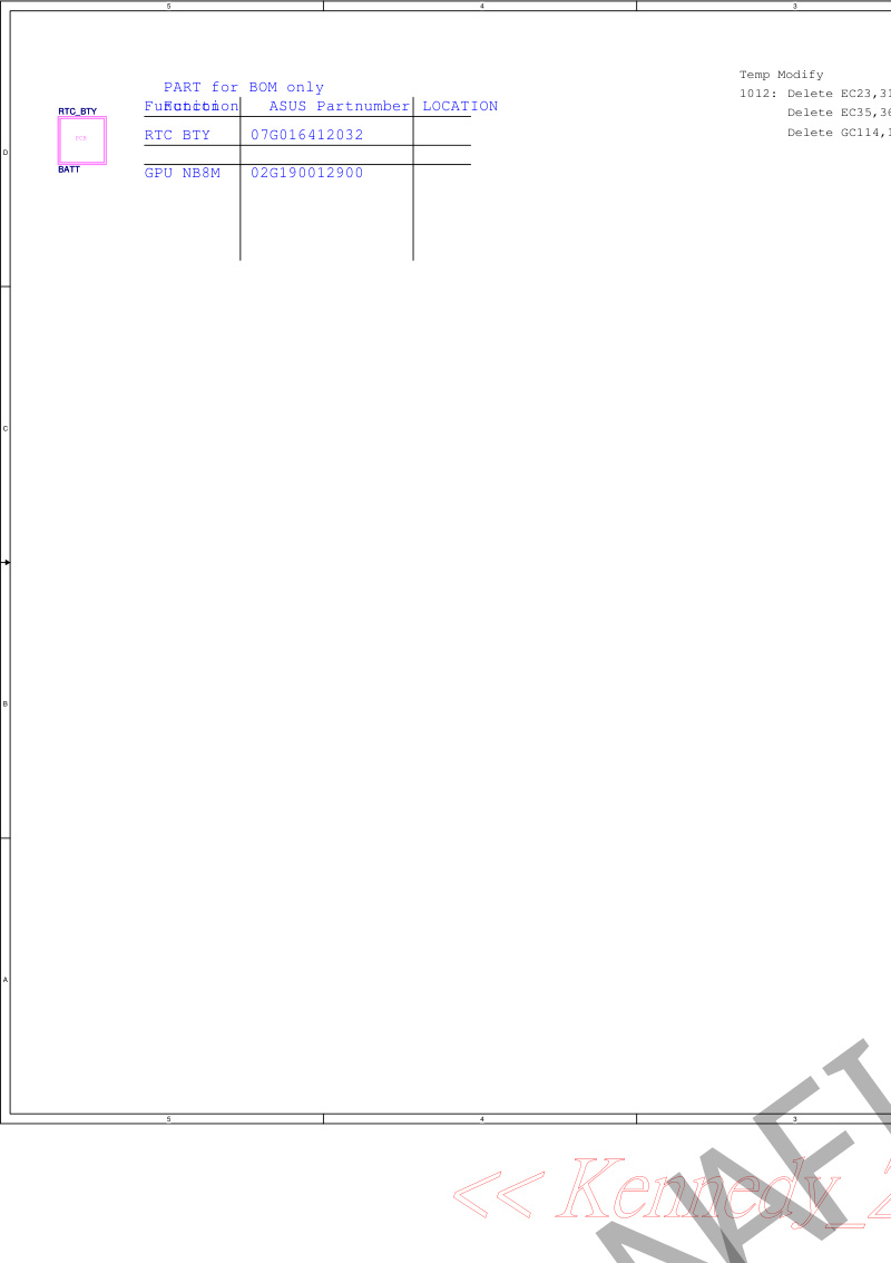
ASUS Z37S/E Schematic Diagram and PCB Layout
Complete schematic diagram and PCB layout documentation for the ASUS Z37S/E motherboard. This technical reference includes full circuit diagrams, component placement maps, and detailed signal routing across all board layers. Essential for technicians performing diagnostics, component-level repair, and system troubleshooting. Covers power delivery circuits, memory interfaces, storage connections, and peripheral signaling paths. Use this documentation alongside the technical specifications to identify component locations, trace signal integrity issues, and verify proper assembly during repair or rework procedures.
Documentation must be downloaded on a computer (PC, Mac, or Linux).
Do not use a smartphone or tablet to download documentation; they generally lack sufficient memory capacity to handle large files, and few users know how to locate the download folder on these devices.
Once downloaded, you can use it right away and even print the pages you need, or use your smartphone in photo mode to translate into the language of your choice: Google Translate
Document Details
- Format
- Size
- 2.3 MB
- Category
- Computers & IT