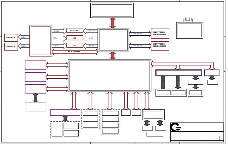
GD1 Main Board Block Diagram and Clock Generator Schematics
Technical schematic documentation for the Sony GD1 main board featuring a comprehensive block diagram that maps the CPU (MEROM), chipset (Crestline, ICH8-M), memory interfaces, PCI-E lanes, USB ports, and card readers. Includes detailed clock generator circuit schematics centered on the ICS9PR363BGLF IC, with complete signal routing, component interconnections, and frequency specifications for repair and maintenance work.
Documentation must be downloaded on a computer (PC, Mac, or Linux).
Do not use a smartphone or tablet to download documentation; they generally lack sufficient memory capacity to handle large files, and few users know how to locate the download folder on these devices.
Once downloaded, you can use it right away and even print the pages you need, or use your smartphone in photo mode to translate into the language of your choice: Google Translate
Document Details
- Format
- Pages
- 36
- Size
- 1.4 MB
- Category
- Computers & IT