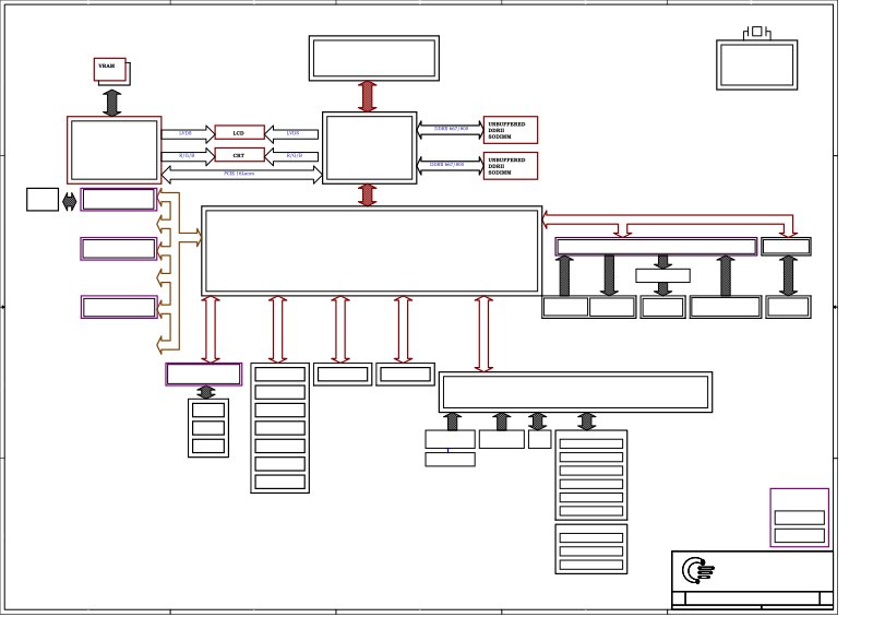
Quanta GD2 Schematic Diagram and Clock Generator
Complete schematic diagrams for the Quanta GD2 laptop motherboard—essential repair and service documentation for technicians working with this Intel Penryn-based platform. The diagrams detail the ICH9-M chipset architecture, Cantiga integrated graphics subsystem, and the critical ICS9LPRS365 clock generator responsible for system timing control. You'll find the detailed CPU block diagram with processor pin assignments and signal flow, Montevina platform memory specifications supporting DDR II at 667 and 800 MHz, full PCI Express lane routing and protocol logic, and comprehensive thermal sensor circuitry with component reference designators and measured signal paths. This schematic is essential for diagnosing motherboard failures, performing component-level repair, troubleshooting power delivery issues, and resolving clock distribution problems on this mobile platform. Use it as your foundation for board-level diagnostics and rework when standard replacement is not feasible.
Documentation must be downloaded on a computer (PC, Mac, or Linux).
Do not use a smartphone or tablet to download documentation; they generally lack sufficient memory capacity to handle large files, and few users know how to locate the download folder on these devices.
Once downloaded, you can use it right away and even print the pages you need, or use your smartphone in photo mode to translate into the language of your choice: Google Translate
Document Details
- Format
- Pages
- 36
- Size
- 1.4 MB
- Category
- Computers & IT