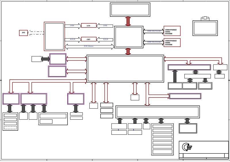
RJ6 Main Board Schematic and Clock Generator Circuit
Complete schematic diagrams and technical reference for the Sony RJ6 main board, a Calistoga chipset-based system featuring the ICS954310/ICS9LPR310 clock generator for CPU clock generation and frequency management. Covers DMI interface architecture, PCIe lane configuration, DDR2 memory controller support, and all peripheral subsystems including the Marvell 88E8055 LAN controller, USB hub connections, SATA controller, PCMCIA interface, and docking connectors. Details voltage regulation circuits across multiple rails, frequency selection lookup tables for clock distribution, and complete signal routing diagrams showing interconnects between chipset, memory, and I/O controllers. Essential for board-level troubleshooting, component-level repair, and understanding the complete system architecture of the RJ6 platform.
Documentation must be downloaded on a computer (PC, Mac, or Linux).
Do not use a smartphone or tablet to download documentation; they generally lack sufficient memory capacity to handle large files, and few users know how to locate the download folder on these devices.
Once downloaded, you can use it right away and even print the pages you need, or use your smartphone in photo mode to translate into the language of your choice: Google Translate
Document Details
- Format
- Pages
- 41
- Size
- 1.6 MB
- Category
- Computers & IT