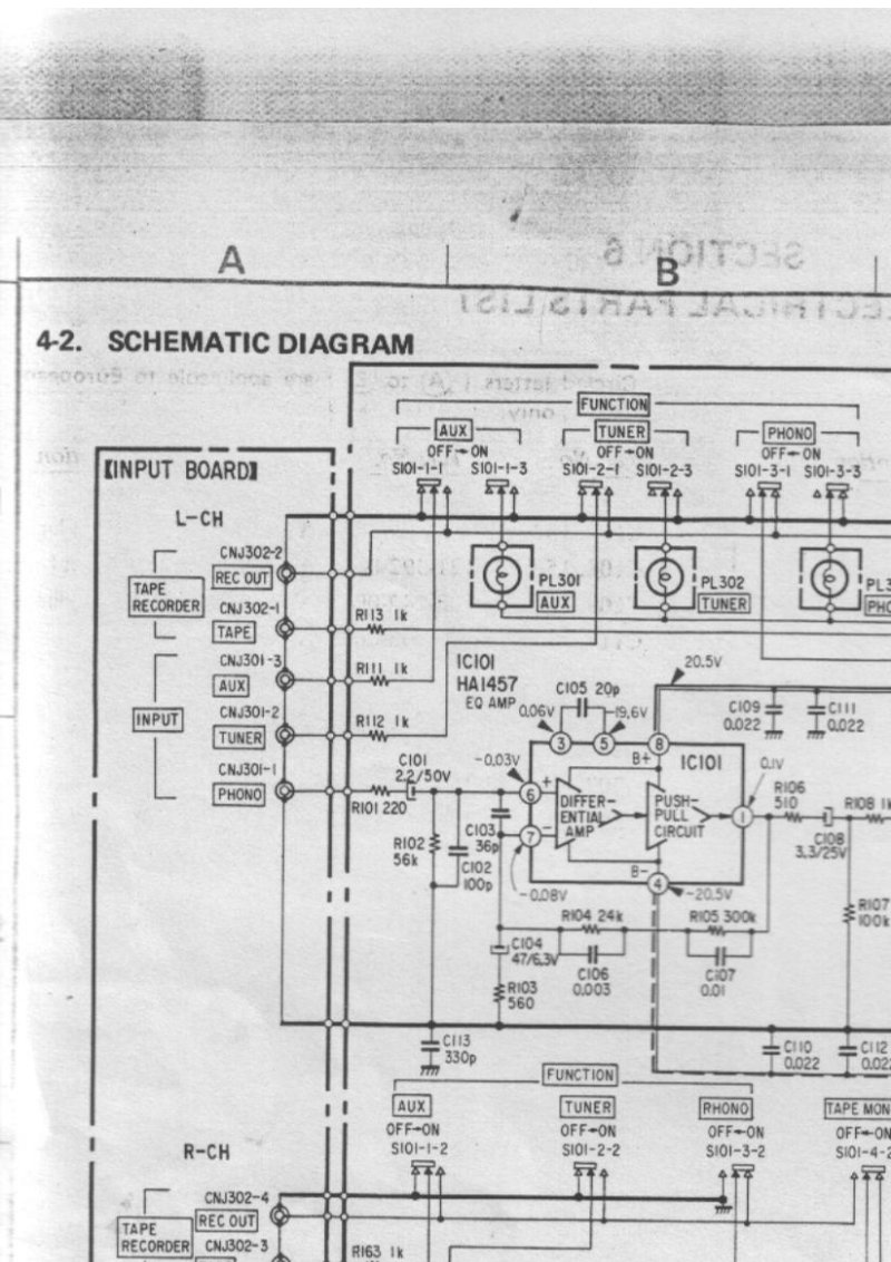
Sony TA-F30 Schematic Diagram
Complete schematic diagram for the Sony TA-F30 integrated amplifier. Provides detailed circuit schematics for the main amplifier board, input stage board, balance control board, tone control board, LED indicator board, and speaker output board, including full component layouts, part values, and signal interconnections. Essential reference material for understanding the amplifier's signal path, power distribution, and audio processing stages. Valuable for troubleshooting, repair work, and service technicians performing maintenance or component-level diagnostics on this classic integrated amplifier model.
Documentation must be downloaded on a computer (PC, Mac, or Linux).
Do not use a smartphone or tablet to download documentation; they generally lack sufficient memory capacity to handle large files, and few users know how to locate the download folder on these devices.
Once downloaded, you can use it right away and even print the pages you need, or use your smartphone in photo mode to translate into the language of your choice: Google Translate
Document Details
- Format
- Pages
- 3
- Size
- 2.8 MB
- Category
- Audio & HiFi